

PRISM Lab
Laboratory for Photonic Research on Innovative Sensing and Monitoring
We are the eyes, ears, and nerves of manufacturing systems.
PRISM Lab is dedicated to advancing manufacturing technologies through the development of next-generation optical monitoring platforms. Our mission is to elevate manufacturing intelligence by enabling real-time monitoring of manufacturing processes and product conditions using advanced optical sensors and analytical methods. PRISM Lab focuses on breakthroughs in micromanufacturing, advanced packaging, additive manufacturing, and silicon photonics. We start small, but we aim big; we committed to illuminating the microscale world through our relentless innovation.

We Focus on:
SEMICONDUCTOR METROLOGY AND QUALITY CONTROL
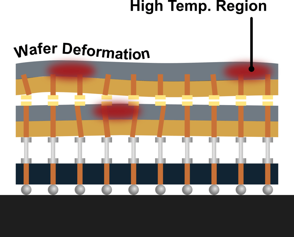
The purpose of this project is to develop optical platforms for in-line and real-time semiconductor metrology and validation. The advanced packaging technology opens a new era of semiconductor integration but also brings challenges: thermal accumulation, thermal and assembly stress, and alignment error, etc. These can reduce the device performance or even cause severe damages. As semiconductor chips move to 3-dimensional, monitoring and validation of semiconductor status and health becomes critical. With our rich experience on optical metrology technology, we will develop optical systems that monitors the 3D temperature and stress distribution, TSV/TGV alignment error, and chip deformation in real-time. With these information, it helps the engineers to optimize chip design and realize a dynamic power control to optimize the chip performance.
LASER ADDITIVE MANUFACTURING
The purpose of this project is to avoid abrupt temperature gradient to realize damage free ceramic additive manufacturing using CO2 lasers. As a cost-effective and high-power laser source, CO2 lasers are ideal choice of ceramic additive manufacturing. However, due to the abrupt local temperature gradient, it is easy to introduce damages in the printed parts or even cause failures. With considering the power delivery processes, the light-mater interaction mechanism, and heat transfer processes, we aim to optimize the temperature field on the product to realize a one-step FDM ceramic 3D printing.

FIBER OPTICAL SENSING FOR PREDICTIVE MANUFACTURING
The purpose of this project is to realize predictive manufacturing by monitoring the real-time product information using a micro-scale fiber optical monitoring platform. With the advanced optical multiplexing technology, multiple product parameters, such as product topography, surface roughness, and surface oxidation, can be monitored with one single optical fiber. Moreover, optical fiber sensors are resistant to erosive environment, highly sensitive, and highly compact, providing us opportunities evaluate the product qualities in real-time.
INTEGRATED PHOTONICS
The purpose of this project is to develop a low-cost and one-step way to manufacture integrated optical circuits. Integrated photonics is a technique to fabricate photonic devices on photonic chips for communication, computation, and sensing purposes. Compared with electronics, integrated photonics has advantages of low power consumption, high speed and bandwidth, and immune to electromagnetic interference. We are developing additive manufacturing technologies to fabricate optical waveguides or photonic structures for fast prototyping with low environmental requirement, low cost, and high speed. This technology will boost the research and application of integrated photonics and unlock the future of optical chips.
